[STM32F3] Hello World with STM32F3 Discovery - Part 3
Checks on the Peripherals
As being discussed in the previous post, we can already use the blocks that is provided by the STM32-MAT support package from STMicroelectronics. Further more we will be checking if we have set the configuration correctly and the register values accordingly.
Learning the effects of a certain configuration will let us understand each parameters of the STM32CubeMX for the STM32F3348Discovery.
Hardware and Software needed:
 |
| Fig. 1 Needed Hardware/Software |
- Matlab/Simulink with Embedded Coder
- Oscilloscope (2 Channels would be sufficient)
- STM32F3348 Discovery Board
- GPIB Cable (depends on your oscilloscope)
- 5 Volts Power Supply
HRTIM TimerB
The key point why we will use the HRTIM timer is that we can be able to achieve higher PWM Frequency. Normally SMPS has around 100kHz to 4MHz of operating frequency. For our case we will be setting the HRTIM Timber B PWM Period to 250kHz and a Repetition IRQ on every 16 or 32 cycles of our PWM. It has also a dead time setting available for us to use, these means that we can be able to set the dead time for the complementary Mosfets that we will be connecting to the HRTIM TB1 and TB2 hence we will be assured that we will not encounter any issues with turning the MOSFETS at the same time (short circuit!).
We can then check the outputs in our STM32F3348Discovery board accordingly. Compare 1 and Compare 2 registers will be used later since it will determine the duty cycle of the PWM, currently it is set to 9216 which half of the Period Register of the HRTIM Timer B (18432). The Repetition Counter is set to 15 where in you need to add one to get the actual repetition counter which is 16.
 |
| Fig. 2 PA11 HRTIM Timer B Output @250kHz and Repetition IRQ |
At this point we can then use the HRTIM Timer B Comp1 value to change the Duty Cycle of the PWM outputs that is connected to the MOSFETS. Timer B Compare 1 is being changed every time the Repetition IRQ is being fired, with the sine wave block with a bias value of the 50% duty cycle to a certain arbitrary value of 2000
DAC (Digital to Analog Conversion)
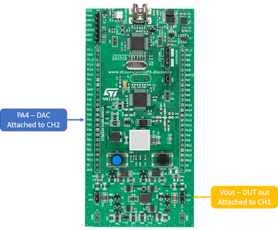
Setting up the DAC is quite simple, what the STM32 DAC simulink block would require is the values that you want to output. Hence puting a value of 0xFFF (12bit) would result to a 3.3 volt. This is based on the Vref that is used, and by default the board should be using a 3.3volt as a reference voltage. I am adding in a DAC to the current setup so that I can be able to monitor the Duty Cycle percentage and the Voltage Output of my Boost Converter on the oscilloscope and use it for the System Identification toolbox to get a transfer function out of it.
3.3 Volt == 4096 == 100% duty cycle
 |
| Fig. 4 Setting up the DAC with conversions |
The output of the sine wave block would be in values range in 0 to 18432 in which we need to convert it to 0 to 4096 range because the DAC only understands 12 bit (2^12 == 4096)
 |
| Fig. 5 DAC output, 3.3Volts == 100% Duty Cycle |
ADC (Analog to Digital Converter) - 12bit
This is the last of the peripherals that we want to check, as stated in the Application Note the ADC is being checked every time the Repetition IRQ is being fired. In order to follow the AN4449
 |
| Fig. 6 Where ADC Block read is placed |
GPIO (General Purpose Input / Output)
As stated in the previous article we just need to set the PA8 to High and PA9 to Low. We just place it in our model.
Summary
Now we have already checked on all the peripherals needed for our objective. To recall the main purpose of this blog series is we can implement a closed loop Boost Converter Switch Mode Power Supply with the STM32F3348 Discovery board. The next steps we will now do is to make an open loop boost converter first. Which means that if ever I set the duty cycle on a certain value (0%-100%) and then check what is the output of our boost converter.


Do you share the source code/project files for this example?
ReplyDelete