[STM32F3] Hello World with STM32F3 Discovery - Part 2
Setting up the hardware:
I wanted to merge the examples provided by STM32-MAT/TARGET (STM32 embedded Target for Matlab/Simulink) and the common use case of System Identification Toolbox, Control System Toolbox and Simulink Control Design Toolbox of Mathworks. This will stream line the capabilities of the support package that the STM32-MAT has provided and the available toolboxes with matlab to be able to develop a Switch Model Power Supply (Boost Converter).References would be on this links:
STM32-MAT Target Support Package
STM32F3348Discovery Website
STM32F3348 Application Note
HRTIM Cookbook
 |
| Fig. 1 The STM32F3348 Discovery board has a buck boost converter on the pcb (Highlighted in red) |
Objective 1: Enable the boost section of the circuit with STM32CubeMX
Based on the documentation of the STM32F3 Application note AN4449 we need to set TA1 (PA8) to high and TA2(PA9) to low. We also need to set the TB1(PA10) to PWM output and TB2(PA11) to the complimentary of the TB1 output.
 |
| Fig. 2 HRTIM output Signals Through Operating Modes |
 |
| Fig. 3 A better picture of the pin configuration |
The STM32CubeMX allows us to configure the MCU conveniently without having any troubles in memorizing all the bit configuration of each registers to set a certain feature or pin of the hardware that we have selected. However we still need to set certain parameters and values to configure completely.
 |
| Fig. 5 STM32CubeMX pin configuration |
Objective 2: HRTIM Configuration
Having already set the PA10 and PA11 as HRTIM PWM outputs (CHB1 and CHB2) we can now proceed to configure our HRTIM registers. I will just focus more on the TABs that has more value rather than explaining each and every one of them.
1. ADC Triggers Configuration this will determine when do we start sampling our ADC pins (Vin/Vout). As set in the figure below the configuration will trigger the ADC1 using the TimerB of the HRTIM when the TimerB compare 2 value has been reached. Later on on the project, we might need to control the TimerB Compare 2 Value so that we will always sample on a certain area on the on time or off time of the PWM.
2. Timer B, setting the HRTIM can be found on the HRTIM cookbook which I have already provided a link at the beginning of the article. We should take note that the Compare 2 Register Value will be changing in the next coming iterations of the program.
 |
| Fig.7 HRTIM Timer B Configuration 1 |
 |
| Fig. 8 HRTIM TIMER B Configuration 2 |
Objective 3: ADC Configuration
As stated in the AN4449 (Application Note) they will be using an ADC Injected conversion node also stated in the ADC documentation for STM32, this mode is intended for use when conversion is triggered by an external event or by
software.
The injected group has priority over the regular channel group. It interrupts the conversion of
the current channel in the regular channel group. This mode can be used to synchronize the conversion of channels to an event. It is
interesting in motor control applications where transistor switching generates noise that
impacts ADC measurements and results in wrong conversions. Using a timer, the injected
conversion mode can thus be implemented to delay the ADC measurements to after the
transistor switching. - STM32™’s ADC modes and their applications
 |
| Fig. 9 ADC Configuration |
Objective 3: DAC Configuration
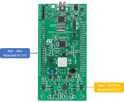
I will be using the DAC output as my voltage value for the duty cycle percentage and it will be connected to an oscilloscope. This will then allow me to capture the data of an open loop boost converter and measuring the output of the converter vs the duty cycle of the PWM output of the HRTIM Timer B
 |
| Fig. 10 DAC configuration |
Summary:
Now we have configured our board to what pin outputs and pin configuration needed for our open loop boost converter. Take note that the next steps would be trying to have a step response to a certain duty cycle percentage with a corresponding voltage output. This will enable us to use System Identification Toolbox of Matlab/Simulink so that we can get the Transfer Function of our boost converter.
From this point we can already use the blocks in Simulink provided that we use the stm32cubeMX configuration file (.ioc)
 |
| Fig. 11 Simulink Blocks Available for use with the configuration ioc file |


Hi, do you have the ioc of this tutorial?
ReplyDeleteI am just starting to learn DSMPS.